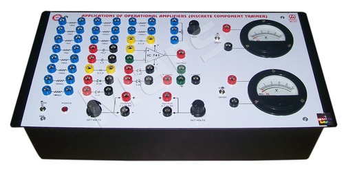
Product Description
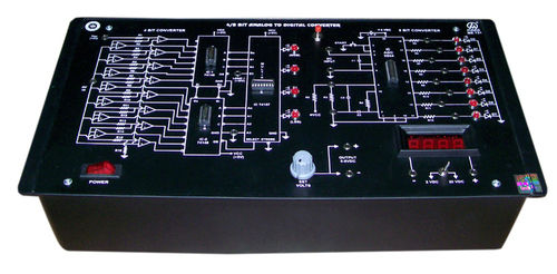
Analog to Digital and Digital to Analog Converter Trainer Kit
FEATURE
IEEE Symbol of all components to be provided on the PCB.
All Components must be visible clearly on the top of the PCB.
It should consist of 8-bit binary weighted and 8-bit ladder type DACare constructed using discrete components
It should consist of 8-bit monolithic DAC having settling time in therange of ns, wide power
supply range, and low power.
It should consist of 8-bit monolithic DAC having settling time in therange of ns, wide power supply range, low power consumption, full scale error +ILSB.
8 bit digital ramp ADC constructed using discrete components should beinclude.
It should provide 12-bit monolithic ADC having conversion time in therange of us, industry standard pin out, wide input range should be including 8onboard switches to provide digital input to DAC.
Should include 8-bitcounter running on external clock frequency tostudy setting time of DAC.
It should consist of built in low power frequency clock generator.
Extensive experimental manual is to be provided with the kit
TECHNICAL SPECIFICATION
On board components
Sine wave generator
Amplitude: OV to 5V
Frequency: 1KHz
Variable DC generator
Voltage Range: -12V to +12V
Digital to Analog converter
8-bit binary weighted DAC
8-bit ladder type D to a converter
8-bit D to A converter using monolithic IC
Analog to Digital converter
8-bit discrete ADC
12-bit successive approximation monolithic IC
Binary counter: 12-bit binary counter with external clock
Output: 12 LEDs to observed ADC output
Interconnection: 2mm connectors.
Power Supply: -12V, +12V, +5V, GND
Versatile Educational Tool for Signal ConversionThis trainer kit empowers students and educators to understand the fundamentals of analog-to-digital and digital-to-analog conversion using industry-standard ICs. Key features like adjustable reference voltages, onboard/external input sources, and test points for all important signals make it an ideal choice for both basic and advanced experiments. Its robust build and safety measures ensure reliable and secure operation.
Enhanced Experimentation and Safety FeaturesWith a fuse-protected power supply and overload protection mechanisms, the kit guarantees safe usage during laboratory sessions. The inclusion of step-by-step switches, push buttons, and a 7-segment digital display enhances the practicality for hands-on demonstration. Additional options like breadboard area panels ensure broader experiment scope for complex studies.
FAQs of Analog to Digital and Digital to Analog Converter Trainer Kit:
Q: How does the Analog to Digital and Digital to Analog Converter Trainer Kit facilitate educational experiments?
A: The trainer kit provides a comprehensive platform for students to perform hands-on experiments in signal conversion, using ADC0804 and DAC0808 ICs. The included instruction manual details various experiments, while test points and adjustable reference voltages enable real-time observation and fine-tuning of results.
Q: What is the process for performing analog to digital conversion using this kit?
A: To perform ADC, users apply an analog input (0 to 5V) to the designated terminal. The ADC0804 IC converts this signal into an 8-bit digital output, which is displayed on the 7-segment panel. Adjustable reference voltage and stepwise operation extend experiment flexibility and accuracy.
Q: When should the onboard signal source be used versus the external input?
A: The onboard signal source is ideal for standardized demonstrations and initial learning, while the external input facilitates advanced experiments, troubleshooting, and real-world applications requiring custom or more diverse signals.
Q: Where are test points provided, and what is their benefit?
A: Test points are conveniently placed across all critical signals within the kit. They grant users direct access to monitor voltages, currents, and signal paths, which is essential for measuring, analyzing, and understanding each stage of the conversion process.
Q: How does the overload protection and fuse provide safety during usage?
A: The built-in overload protection and fuse secure the kit from electrical surges and excessive currents, preventing component damage and ensuring the users safety throughout experiment sessions.
Q: What features support advanced experimentation and study?
A: Advanced study is supported through compatibility with multiple ADC/DAC ICs, optional breadboard panel area, adjustable reference voltage, and the capability for both single and multi-channel operation, allowing exploration of complex designs and conversion mechanisms.